| Power System Blockset | Search Help Desk |
| Mosfet | Examples See Also |
Library
Power Electronics LibraryDescription
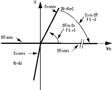
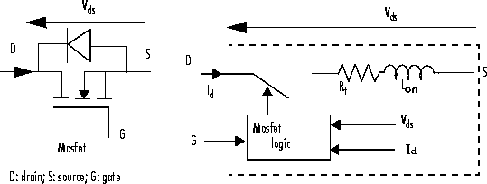
The Mosfet block turns on when the drain-source voltage is positive and a positive signal is applied at the gate input (G >0).
With a positive current flowing through the device, the Mosfet block turns off when the gate input becomes zero. If the current Id is negative (Id flowing in the internal diode) and the gate signal is zero (G = 0), the Mosfet block turns off when the current Id becomes zero (Id = 0).
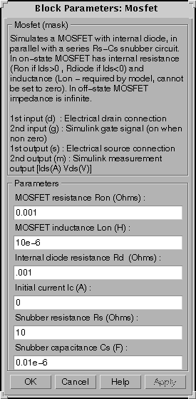
Note that the on-state resistance Rt depends on the drain current direction:Parameters and Dialog Box
Inputs and Outputs
The first input and output are the Mosfet connection to drain (d) and source (s). The second input (g) is a logical Simulink signal applied to the gate. The second output is a Simulink measurement vector [Id, Vds] returning the Mosfet current and voltage.Assumptions and Limitations
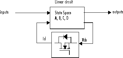
The Mosfet block implements a macro-model of the real Mosfet device. It does not take into account either the geometry of the device or the complex physical processes [1]. In the Simulink representation, the Mosfet is modeled as a nonlinear element interfaced with the linear circuit as shown below.To avoid an algebraic loop, the Mosfet inductance Lon cannot be set to zero. Each Mosfet adds an extra state to the electrical circuit model. Since the Mosfet is modeled as a current source, it cannot be connected in series with an inductor, a current source, or an open circuit, unless a snubber circuit is used.
You must use a stiff integrator algorithm to simulate circuits containing mosfets.ode23tb and ode15s usually gives best simulation speed.
Example
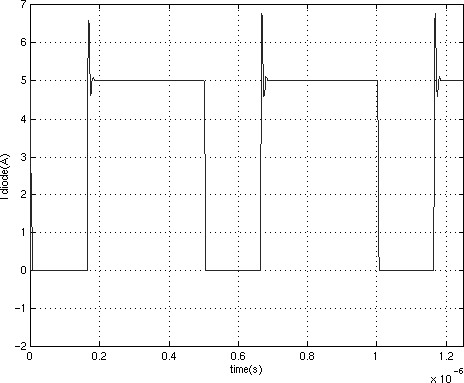
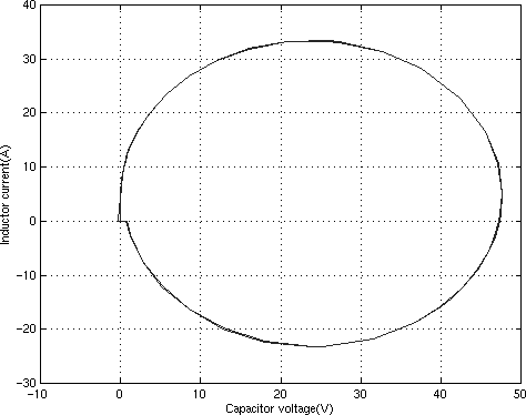
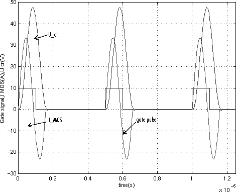
The following example illustrates the use of the Mosfet block in a Zero-Current-Quasi-Resonant Switch converter. In such a converter, the current produced by the Lr-Cr resonant circuit flows through the device, thus causing it to turn on and off at zero current [1]. The switching frequency is 2 MHz and the pulse width is 72 degrees (duty cycle: 20%). This example is available in thepsbmosconv.mdl file
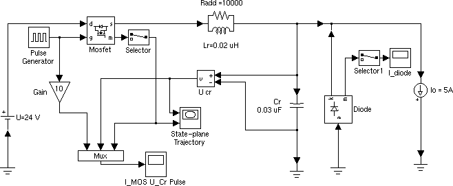
Run the simulation and observe the capacitor voltage, the mosfet current, the gate pulse signal, the diode current, and the state-plane trajectory (inductor current versus capacitor voltage).
References
[1] Mohan N., Power Electronic, Converters, Applications and Design, John Wiley & Sons, Inc., New York, 1995.See Also
Diode, GTO, Ideal Switch, Thyristor