| Power System Blockset | Search Help Desk |
| GTO | Examples See Also |
Implement a GTO-thyristor model
Library
Power Electronics LibraryDescription
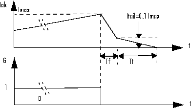
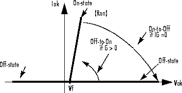
The GTO-thyristor turns on when the anode-cathode voltage is greater than Vf and a positive pulse signal is present at the gate input (G>0). When the gate signal is set to zero, the GTO starts to block, but its current does not stop instantaneously.
Since the current extinction process of a GTO-thyristor contributes significantly to the turn-off losses, the turn-off characteristic is built into the model. The current decrease is approximated by two segments. When the gate signal becomes zero, the current Iak first decreases from the value Imax (value of Iak when the GTO starts to open) to Imax/10, during the fall time (Tf), and then from Imax/10 to zero during the tail time (Tt). The GTO-thyristor turns off when the current Iak becomes zero. The latching and holding currents are not considered.
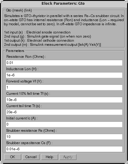
Vf, Ron and Lon are the forward voltage drop while in conduction, the forward conducting resistance, and the inductance of the device, respectively.
The GTO-thyristor block also contains a series Rs-Cs snubber circuit which is usually connected in parallel with the device. Due to modeling constraints, the inductance Lon cannot be set to zero. You can specify a snubber which is purely resistive (Cs = Inf) or purely capacitive (Rs=0). If you specify either Rs=Inf or Cs=0, the snubber is eliminated and it disappears on the GTO-thyristor icon.
The initial current Ic is usually set to zero, so that the simulation is started with the GTO-thyristor blocked. However, you may specify an Ic value corresponding to a particular state of the circuit. In such a case, all states of the linear circuit must be set accordingly. Initializing all states of a power-electronic converter is a complex task. Therefore, this option is useful only with simple circuits.
Dialog Box
Inputs and Outputs
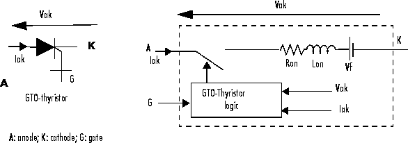
The first input and output are the GTO-thyristor terminals connected respectively to anode (a) and cathode (k). The second input (g) is a Simulink signal applied to the gate. The second output (m) is a Simulink measurement output vector [Iak, Vak] returning the GTO-thyristor current and voltage.Assumptions and Limitations
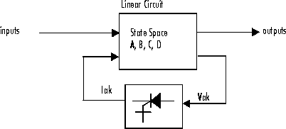
The GTO-thyristor block implements a macro-model of a real GTO-thyristor, and it does not take into account either the geometry of the device or the underlying physical processes of the device [1]. The GTO-thyristor requires a continuous application of the gate signal (G>0) in order to be in the on-state (with Iak>0). The latching current and the holding current are not considered. The critical value of the derivative of the re-applied anode-cathode voltage is not considered. The GTO-thyristor is modeled as a nonlinear element interfaced with the linear circuit, as shown below.To avoid an algebraic loop, the GTO-thyristor inductance Lon cannot be set to zero. Each GTO-thyristor adds an extra state to the electrical circuit model. The GTO-thyristor is modeled as a current source. It cannot be connected in series with an inductor, a current source, or an open circuit, unless a snubber circuit is used.
You must use a stiff integrator algorithm to simulate circuits containing GTO-thyristors.ode23tb and ode15s usually give best simulation speed.
Example
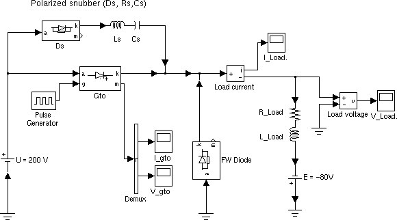
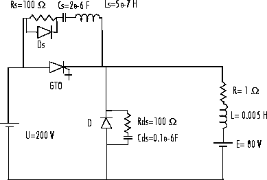
The following example illustrates the use of the GTO-thyristor block in a buck converter topology. The basic polarized snubber circuit is connected across the GTO. The snubber circuit consists of a capacitor Cs, a resistor Rs, and a diode Ds. The parasitic inductance Ls of the snubber circuit is also taken into consideration. The parameters of the GTO are those found in the Dialog Box section, except for the internal snubber, which is out of service (Rs=Inf Cs=0). The switching frequency is 1000 Hz and the pulse width is 216 degrees (duty cycle 60%). This example is available in the psbbuckconv.mdl file.
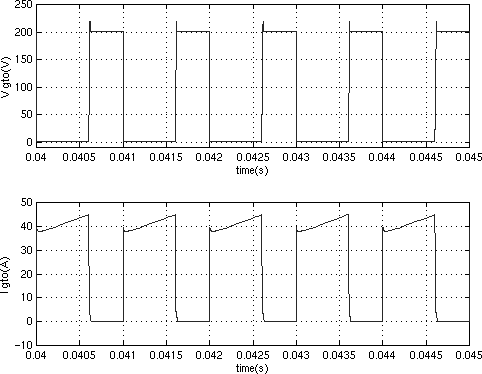
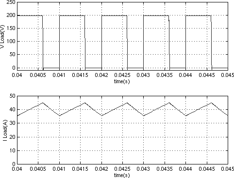
 Run the simulation and observe the GTO voltage and current as well as the load voltage and current.
References
[1] Mohan N., Power Electronic, Converters, Applications and Design, John Wiley & Sons, Inc., New York, 1995See Also
Diode, Thyristor, Mosfet, Ideal Switch