| Power System Blockset | Search Help Desk |
| Thyristor | Examples See Also |
Library
Power Electronics LibraryDescription
The Thyristor block also contains a series Rs-Cs snubber circuit, which is usually connected in parallel with the thyristor.You can specify a snubber which is purely resistive (Cs = Inf) or purely capacitive (Rs=0). If you specify either Rs=Inf or Cs=0, the snubber is eliminated and it disappears on the thyristor icon.
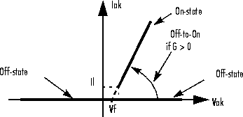
The static VI characteristic of this model is shown in the figure that follows.The thyristor turns on when the anode-cathode voltage is greater than Vf and a positive pulse signal is present at the gate input (G>0). The pulse height must be greater than zero and last long enough to allow the thyristor anode current to become larger than the latching current Il.
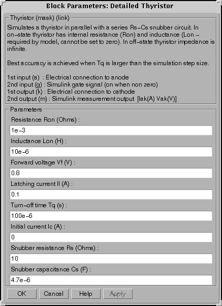
The thyristor turns off when the current flowing in the device becomes zero (Iak=0) and a negative voltage appears across the anode and cathode for at least a period of time equal to the turn-off time Tq. If the voltage across the device becomes positive within a period of time less than Tq, the device will turn on automatically even if the gate signal is low (G = 0) and the anode current is less than the latching current. Furthermore, if during turn on, the device current amplitude stays below the latching current level specified in the dialog box, the device turns off after the gate signal level becomes low (G = 0). The turn-off time Tq represents the carrier recovery time: it is the time interval between the instant the anode current has decreased to zero and the instant when the thyristor is capable of withstanding positive voltage Vak without turning on again. Simplified Model and Detailed ModelTo optimize simulation speed, two models of thyristors are available: the simplified model and the detailed model. For the simplified thyristor model, the latching current Il and recovery time Tq are assumed to be zero.
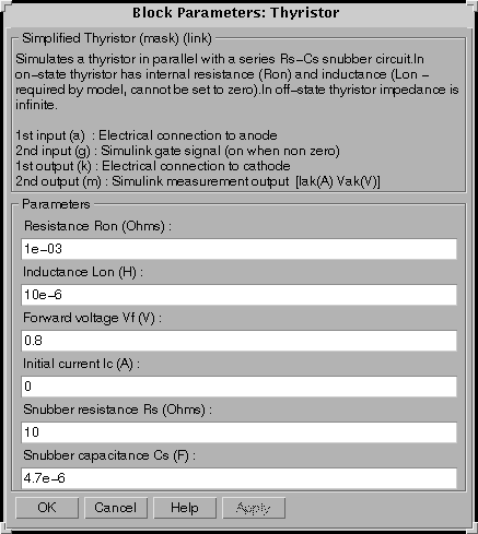
Enter the thyristor parameters Ron, Lon, and Vf and the Rs-Cs snubber parameters in the dialog box. Due to modeling constraints explained below, the inductance Lon cannot be set to zero. The initial current Ic flowing in the thyristor is usually set to zero so that the simulation is started with the thyristor blocked. However, you may specify an Ic value corresponding to a particular state of the circuit. In such a case all states of the linear circuit must be set accordingly. Initializing all-states of a power-electronic converter is a complex task. Therefore, this option is useful only with simple circuits. For applications where the thyristor is used in general purpose rectifier circuits fed by a voltage source at a frequency of 50 or 60 Hz, the typical parameters values specified in the dialog box can be used.Dialog Boxes
Simplified Thyristor Dialog BoxInputs and Outputs
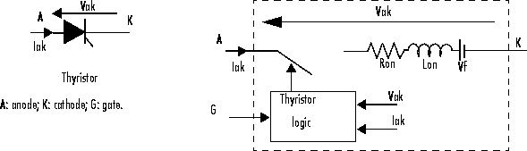
The thyristor icon consists of two inputs and two outputs. The first input and output are the thyristor terminals connected respectively to anode (a) and cathode (k). The second input (g) is a Simulink logical signal applied to the gate (G). The second output (m) is a Simulink measurement output vector [Iak, Vak] returning the thyristor current and voltage.Assumptions and Limitations
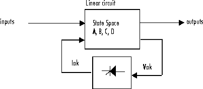
The Thyristor block implements a macro-model of the real thyristor. It does not take into account either the geometry of the device or complex physical processes that model the behavior of the device [1-2]. The forward breakover voltage and the critical value of the derivative of the reapplied anode-cathode voltage are not considered by the model. In the Simulink representation, the thyristor is modeled as a nonlinear element interfaced with the linear circuit as shown below.Therefore, in order to avoid an algebraic loop, the thyristor inductance Lon cannot be set to zero. Each thyristor adds an extra state to the electrical circuit model. As the thyristor is modeled as a current source, it cannot be connected in series with an inductor, a current source or an open circuit unless a snubber circuit is used.
You must use a stiff integrator algorithm to simulate circuits containing thyristors.ode23tb and ode15s usually give best simulation speed.
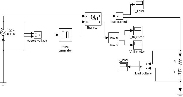
Example
Single pulse thyristor rectifier feeding a RL load. The gate pulses are obtained from a pulse generator synchronized on the source voltage. The circuit is available in thepsbthyristor.mdl file. The following parameters are used:
R=1 ; L=10mH; Thyristor block: Ron=0.001 , Lon=1e-5 H, Vf=0.8 V, IC=0 A, Rs=20 , Cs=4e-6 F. Simulation parameters:
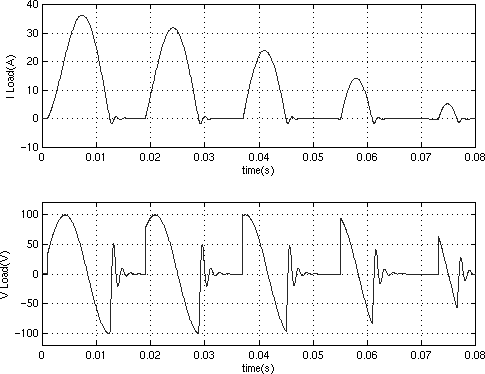
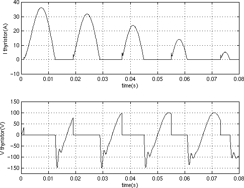
 ode15s; Relative tolerance: 1e-3; Absolute tolerance: 1e-3.The firing angle is varied by the Pulse Generator block synchronized on the voltage source. Run the simulation and observe the load current and voltage, and the thyristor current and voltage.
Load current and voltage:References
[1] Rajagopalan, V., Computer-Aided analysis of Power Electronic Systems, Marcel Dekker, Inc., New York,1987. [2] Mohan, N., Power Electronic, Converters, Applications and Design, John Wiley & Sons, Inc., New York, 1995.See Also
Diode, Mosfet, GTO, Ideal Switch