| Power System Blockset | Search Help Desk |
| Ideal Switch | Examples |
Implement an Ideal Switch model
Library
Power Electronics LibraryDescription
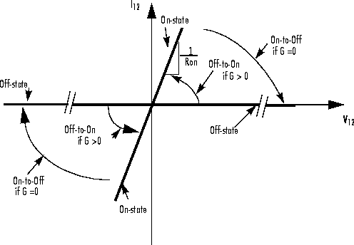
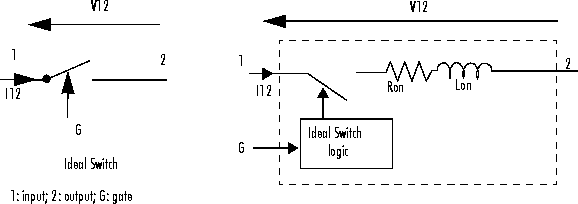
The Ideal Switch is fully controlled by the gate signal (G>0 or G=0). It has the following characteristics:
Dialog Box
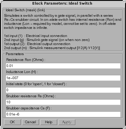
Because of modeling constraints explained in the Assumptions and Limitations section, the inductance Lon cannot be set to zero. If the switch initial state is set to 1 (closed), the states of the linear circuit are automatically initialized so that the simulation starts in steady-state.
Inputs and Outputs
The first input (1) and output (2) are the Ideal Switch electrical connections. The second input (g) is a Simulink signal applied to the gate. The second output (m) is a Simulink measurement output vector [I12,V12] returning the Ideal Switch current and voltage.Assumptions and Limitations
It can happen that the switch is connected across a capacitor. Depending on the values of the capacitor, switch resistance and inductance, high frequency poorly damped current and voltage oscillations can be produced when the switch closes if the Ron-Lon parameters are not properly selected. This will result in a slow simulation speed. A good practice is to achieve a damping factor of z>0.5 for the Ron-Lon-C circuit. This condition is obtained when For example, with Ron =0.01
  and C= 1e-6 F, you should select Lon
 1e-10 H.
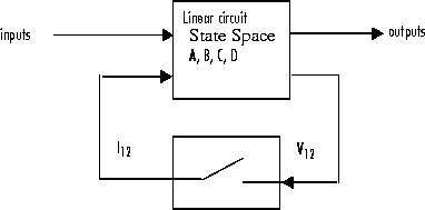
The Ideal Switch is modeled as a nonlinear element interfaced with the linear circuit, as shown below.
1e-10 H.
The Ideal Switch is modeled as a nonlinear element interfaced with the linear circuit, as shown below.To avoid an algebraic loop, the Ideal Switch inductance Lon cannot be set to zero. Each Ideal Switch adds an extra state to the electrical circuit model. The Ideal Switch is modeled as a current source. It cannot be connected in series with an inductor, a current source or an open circuit, unless a snubber circuit is used.
You must use a stiff integrator algorithm to simulate circuits containing Ideal Switches.ode23tb and ode15s usually give best simulation speed.
Example
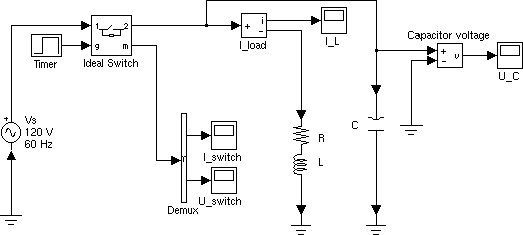
An Ideal Switch is used to switch an RLC circuit on an AC source (60 Hz). The switch, which is initially closed, is first open at t=36 ms and then closed at t=100 ms. As the switch is used to switch a capacitor, its inductance Lon has been set to a very small value to satisfy the condition. This example is available in the
 psbswitch.mdl file.
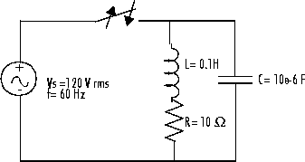
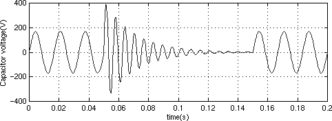
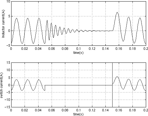
Run the simulation and observe the inductor current, the switch current and the capacitor voltage. Notice the high frequency overvoltage produced by inductive current chopping.
References
[1] N. Mohan, Power Electronic, Converters, Applications and Design, John Wiley & Sons, Inc., New York, 1995.