The vital component of any spectrometer is its spectral dispersing device - a physical means of spreading radiation composed of differing photon energies (thus a range of frequencies or their inverse, wavelengths) laterally into a stretched out linear display. The simplest device is an optical glass prism whose cross-section is a triangle. A polychromatic light (or non-visible radiation) beam first strikes one side of the triangle. At this interface, the rays with different wavelengths will be bent according to their response to the refractive power of the glass. The degree of bending varies with wavelength; this means that the index of refraction also differs for the range of wavelengths (for example, in crown glass the index is 1.528 for violet and 1.514 for red). If the beam strikes one side of a right triangle prism at a right angle, it continues in the same direction but is slowed down and then becomes bent to differing extents as it emerges at the slant (hypotenuse) edge on the opposite side; if the prism is oriented with the hypotenuse face as its base (parallel to the incoming light beam), the beam will first meet a slant face, then bend, and the now dispersed light will again meet the second slant face and will bend further. The net effect is to spread out the (visible) light rays according to their effective indices of refraction into a continuous geometric color pattern that forms the wavelength abscissa of a spectral plot.
A diffraction grating disperses light according to a different mechanism. The grating can be metal or glass on which are ruled (cut) fine grooves of straight, parallel lines that are extremely close-spaced (e.g., 15000 per inch, so that the spacing between pairs is roughly equivalent to the wavelengths in the VNIR). Each line, analogous to a slit, causes polychromatic light to be diffracted (bent) at angles that depend on wavelength. For the array of close-spaced lines (each pair separated by a distance d), the Bragg equation can be applied: n lamda (wavelength) = d sin theta (angle of bending), where n refers to simple integers (1,2,3...) that establish orders (overtones). Thus, a ray of light striking the grating will undergo spreading at various angles according the wavelengths contained within it. Some wavelengths will have larger numbers of photons (more intense) than others, so that the plot of reflected light energies can be recast as reflectance versus wavelength, hence yielding the type of spectral curves we have examined in the previous two pages.
(An emission spectrometer used to analyze material compositions takes light of discrete wavelengths representing excitation states of different chemical elements through a slit and then a prism or diffraction grating onto a recording medium such as a photographic plate, causing wavelength-dependent bending that reproduces a series of lines (repeated images of the slit) at varied spacings whose wavelengths can be measured, thus allowing idenfication of the particular elements in a sample that is usually heated in a flame or electric arc to force electrons into higher energy states [light of given wavelengths is emitted according to the quantized energy involved in the transition to a lower state - remember Planck's equation E = hv, where v is the frequency, discussed in the Tutorial Introduction Section]).
A stationary reflectance spectrometer looking through a collimating lens at a ground scene will just break down the light into wavelengths emanating from the fixed view. The problem compounds when the scene moves past the lens (or the spectrometer swings across the scene). Using older types of detectors, there isn't enough time to record the ever changing field of view, that is, the electronics can't sample the dispersed light fast enough to resolve it into the closely-spaced wavelengths needed to construct a spectral curve. Instead, the light must be recorded as broad bands, in the manner of Landsat-type scanners.
The ability to develop a scanning spectrometer that can sweep across moving terrain while sampling at narrow wavelength intervals had to await a technological breakthrough. This came with the advent of Charge-Coupled Detectors (CCD's). A CCD is a microelectronic semi-conducting metal chip that serves to detect light. Radiation will produce an electron charge on the chip in proportion to the number of photons received (governed by intensity and exposure time). The charge must be rapidly removable, resetting the CCD for the next influx of photons (such as those coming from an adjacent part of the scene being sampled).
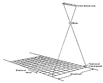
A chip is extremely small in size (tens of micrometers). It is made of some light-sensitive material such as the silicon used in computer microchips. It is normally mounted with hundreds of other tiny chips arranged in a linear or a two-dimensional array. Consider a linear array of, say, 2000 chips per inch. Allow light gathered through lenses to strike the array simultaneously from its one end to the other. Each chip will receive light from some small part of the scene; the next chip will get its light from the ground or air located in a position next to the previous target site, and so on until a line of finite width and length on the ground has been sampled. The chip, accruing a charge representative of the photon batch sent by a "piece of real estate", is in effect a pixel that defines a spatial resolution which depends on the chip size and the height (distance) of the chip array above (from) the scene being scanned. After an instant of dwell time over the target, all of the chips are discharged sequentially (producing a signal stream) to reset the detectors. The chips have a high signal to noise (S/N) ratio which allows in the brief moment enough buildup of electrons, coupled with gain amplification, to yield usable signals. After a single exposure, as the array has moved on a small distance, the process is repeated for the next line of real estate (ground target). The advance of the linear array, likened to the forward motion of a wide "pushbroom", will generate a succession of varying electronic signals that can be converted into an image in which the range of grey levels relate to the signal changes.
A variant of this is the two-dimensional array which receives light from rectangular ground scenes that is captured simultaneously by multiple lines of chips. Or, another mode uses a rocking or rotating mirror to sweep across the array.
The sensor that utilizes CCD elements can be multispectral if it uses several array devices each dedicated to a wavelength band whose width is determined by a bandpassing filter. SPOT's sensor uses CCD arrays and red, green, and infrared filters to create its multispectral data set.
But, these broad band sensors do not provide hyperspectral data, that is, they do not sample the spectrum in narrow intervals. To accomplish this, the sensor detector must consist of many parallel rows of chips, each dedicated to a narrow wavelength interval, that can be sampled (CCDs discharged) extremely rapidly. Imagine a two-dimensional array with several hundred chips across its width and 200 or so stacked successively along its front-back length. Let the light enter the sensor through a telescope or focusing lens, impinge against a moving mirrored surface, and then pass through a diffraction grating which disperses the light over a spectral range in the direction of the array length (which is also the same direction of forward motion of the sensor). At one instantaneous position of the mirror, the light from the ground activates the first pixel chip in the width array and at the same time does so for the succession of wavelengths in the chip array downlength (the spectral dimension). That lengthwise linear array is sampled electronically. Now the mirror moves widthwise to the next ground spot and the light from it repeats its spectral dispersion lengthwise. The mirror continues progressively to complete the equivalent of one ground sweep. While this happens, the sensor moves on to look at the next ground position and the whole scanning-dispersing process is duplicated. As the instrument proceeds along its flight path or orbit, the final result is a vast collection of data that has both spatial and hyperspectral inputs. From the data set, images can be constructed using individual narrow spectral bands associated with small plots on the ground. Or, spectral data for any pixel position across the width can be tied to the wavelengths sampled lengthwise to allow a spectral curve to be plotted for that piece of the surface (or, with special modifications, for the atmosphere if that is the target being sensed).
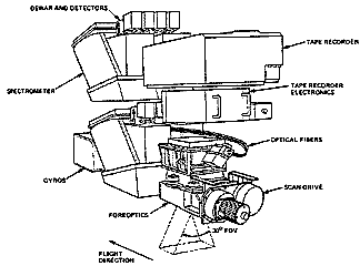
This, in a general way, describes how AVIRIS and other Hyperspectral Imaging Spectrometers operates. JPL's AVIRIS uses diffraction gratings with two sets of CCD arrays, one using silicon chips to sense in the Visible Range and the other In-Sb (Indium-Antimony) chips for wavelengths in the NIR-SWIR range. The detectors must be cooled by liquid nitrogen for optimum performance. There are 224 detectors (channels) in the spectral dimension, extending over a range of 0.38 to 2.50 µm. This leds to a spectral resolution for each chip of 0.01 µm. By choice the units adopted for reporting hyperspectral data is the nanometer (nm); 1000 nm = 1 µm. The resolution stated this way is 10 nm, and the range of coverage is 380 to 2500 nm. AVIRIS gathers its light through a 30° field of view, sending radiation to the 614 individual CCD's in the width (across flight) direction. An oscillating mirror scans the scene and sends the incoming radiation to sweep across the array. The spatial resolution derived from this depends on platform height. A typical mission, mounting AVIRIS on a NASA aircraft (ER-2), produces a spatial resolution around 20 meters but that can be varied to as good as 5 meters by flying at lower altitudes which, of course, narrows the width of ground coverage.
This is what AVIRIS looks like:
And this is an example of an AVIRIS spectral curve for a single pixel:
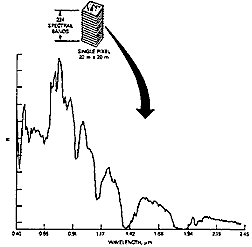
The stacking under the pixel at top is meant to denote the multiple 224 10 nm channels whose values were plotted to attain this curve.
Another way to visualize the relation between an image developed in the usual color compositing manner, but using just three 10 nm data values at different wavelengths, and the spectral variations over the interval sampled is to depict this as a Hyperspectral Cube:
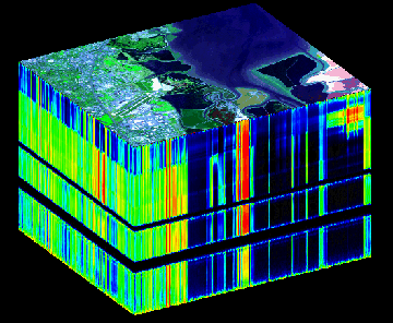
Here, the top of the cube is a quasi-natural color image made from the reflectances associated with three narrow spectral channels in the visible. On the left and right front sides are color representations of the spectra for each of the pixels located along the lines joining the top image with the spectral dimensions. The top corresponds to the low end of the spectrum and the bottom the high end. Blacks through purple and blue are assigned to low reflectances; yellows through red and then white denote high reflectances. The area shown was imaged by AVIRIS during an aircraft flight over the southern part of San Francisco Bay. Landing strips at Moffett Field next to NASA's Ames Research Center locate that part of the image within Mountain View, Calif.
Since AVIRIS, many other imaging spectrometers have been constructed and put online. A list of most of these, in tabular form, can be inspected, if you choose.
One of these is HYDICE, developed by the Navy, for aerial use. It has 210 channels, each with a spectral resolution of ~10 nm, extending from 413 to 2504 nm. It uses a prism as the spectral dispersion device. The spatial dimension is defined by a row of 320 pixels. When flown at low altitudes, HYDICE yields images with resolutions approaching 1 meter. Another instrument, developed in Europe, is DAIS, the Digital Airborne Imaging Spectrometer, which uses a diffraction grating to obtain spectral coverage between 450 and 2500 nm. Its 72 channels pick up radiation in three spectral intervals: 400-1200 nm (bandwidth 15-30 nm); 1500-1800 nm (bandwidth 45 nm); 2000-2500 nm (bandwidth 20 nm); the gaps coincide with atmospheric absorption bands. As separate sensors using the same optics, it also has a single broad band channel between 3000-5000 nm and 6 channels that operate within parts of the 8000-14000 nm interval; these provide important information on thermal emissions from ground objects. Flown low, it provides 1 meter resolution imagery for strips a few kilometers wide.
For most systems, the diffraction grating or the prism accomplishes the dispersion but other techniques of separating the spectrum include interference filters, acoustical-optical filters, liquid crystal tunable filters, Michelson interferometers, Fourier Transform interferometers, and multi-order etalons. Chips made of mercury-cadmium-tellurium (MCT) or platinum silicide are sensitive to certain usuable wavelength intervals.
Code 935, Goddard Space Flight Center, NASA
Written by: Nicholas M. Short, Sr. email: nmshort@epix.net
and
Jon Robinson email: Jon.W.Robinson.1@gsfc.nasa.gov
Webmaster: Bill Dickinson Jr. email: rstwebmaster@gsti.com
Web Production: Christiane Robinson, Terri Ho and Nannette Fekete
Updated: 1999.03.15.